Connector - IDE InternalIDE=Integrated Drive Electronics.
Developed by Compaq and Western Digital.
Newer version of IDE goes under the name ATA=AT bus Attachment.40 PIN IDC MALE at the controller & peripherals.
40 PIN IDC FEMALE at the cable. 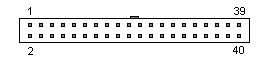 | (at the cable) | 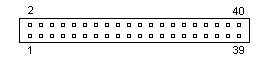 | (at the controller & peripherals) |
| Pin | Name | Direction | Description |
|---|
| 1 | /RESET | Output | Reset | | 2 | GND | --- | Ground | | 3 | DD7 | --- | Data 7 | | 4 | DD8 | --- | Data 8 | | 5 | DD6 | --- | Data 6 | | 6 | DD9 | --- | Data 9 | | 7 | DD5 | --- | Data 5 | | 8 | DD10 | --- | Data 10 | | 9 | DD4 | --- | Data 4 | | 10 | DD11 | --- | Data 11 | | 11 | DD3 | --- | Data 3 | | 12 | DD12 | --- | Data 12 | | 13 | DD2 | --- | Data 2 | | 14 | DD13 | --- | Data 13 | | 15 | DD1 | --- | Data 1 | | 16 | DD14 | --- | Data 14 | | 17 | DD0 | --- | Data 0 | | 18 | DD15 | --- | Data 15 | | 19 | GND | --- | Ground | | 20 | KEY | --- | Key | | 21 | n/c | --- | Not connected | | 22 | GND | --- | Ground | | 23 | /IOW | Output | Write Strobe | | 24 | GND | --- | Ground | | 25 | /IOR | Output | Read Strobe | | 26 | GND | --- | Ground | | 27 | IO_CH_RDY | Input | | | 28 | ALE | Output | Address Latch Enable | | 29 | n/c | --- | Not connected | | 30 | GND | --- | Ground | | 31 | IRQR | Input | Interrupt Request | | 32 | /IOCS16 | | IO ChipSelect 16 | | 33 | DA1 | Output | Address 1 | | 34 | n/c | --- | Not connected | | 35 | DA0 | Output | Address 0 | | 36 | DA2 | Output | Address 2 | | 37 | /IDE_CS0 | Output | (1F0-1F7) | | 38 | /IDE_CS1 | Output | (3F6-3F7) | | 39 | /ACTIVE | Output | Led driver | | 40 | GND | --- | Ground |
Note: Direction is Controller relative Devices (Harddisks). Contributors: Joakim ?gren, Dan Williams Source:
? Copyright © The Hardware Book Team 1996-2001.
May be copied and redistributed, partially or in whole, as appropriate.
Document last modified: 2001-06-07 | 
